
Schematic Capture
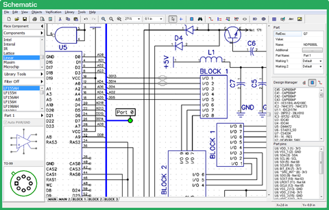
Multi-Level Hierarchical Schematics
Schematic Capture is an advanced circuit design tool with support of multi-sheet and multi-level hierarchical schematics. This module of DipTrace delivers a number of features for visual and logical pin connections. Cross-module management ensures that principal circuits can be easily converted to PCB, back annotated, or imported/exported from other EDA, CAD, and netlist formats. Verification and SPICE export for simulation allow for full project analysis.more details…
3D Modeling
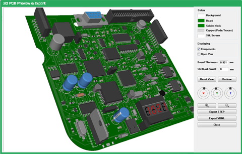
Real-Time 3D Preview & Export
DipTrace PCB Layout module includes real-time 3D preview & export feature. It shows the model of manufactured printed circuit board with all components installed. You can rotate the board in three axes, zoom in and out in real time, change colors of the board, copper areas, solder mask, silkscreen, and background. 3D preview works on all stages of the design. Board can be exported to STEP or VRML 2.0 formats for mechanical CAD modelling. More than 7,500 3D models of PCB packages are supplied for free. Externally designed 3D models in *.wrl, *.step, *.iges, and *.3ds formats can be uploaded and attached to patterns in Pattern Editor or PCB Layout.more details…
Library Creation
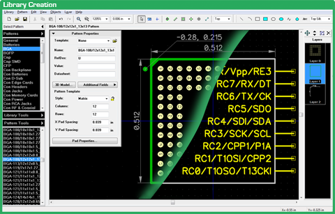
Smart Component Management
DipTrace is always up-to-date; we continuously expand component libraries and bring innovations directly to you. The standard library set already includes more than 140,000 components and 15,200 patterns. Pattern and Component Editors allow you to design new components with custom templates, bulk pin naming, pad renumbering, and bus management instruments, which significantly increase the working speed. Importing libraries and 3D models from various formats adds even more engineering capabilities. Component and Pattern library verifications ensure an error-free design environment from the early beginning.more details…
PCB Layout
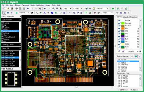
Advanced Routing Capabilities
PCB Layout is a high-level engineering tool for board design featuring smart manual routing of high-speed and differential signals, shape-based autorouter, advanced verification, and wide import/export capabilities. Design requirements are defined by net classes, class-to-class rules, and detailed settings by object types for each class or layer. DipTrace features design process with real-time DRC, which reports errors on the fly before actually making them. The board can be previewed in 3D and exported for mechanical CAD modeling. Design Rule Check with in-depth detailing, Net Connectivity verification, and comparing to source schematic ensure maximum quality of the final product.more details…